Introduction: Experience is the Best Teacher in PCB Design
After two decades in the PCB design industry, I can confidently say that true expertise doesn’t come from textbooks—it comes from trial, error, and real-world problem-solving. Designing PCBs isn’t just about connecting circuits correctly; it’s about ensuring reliability, efficiency, and manufacturability.
If you’re new to PCB design or even an experienced engineer looking to refine your skills, here are the hard-earned lessons I wish I had known earlier.
1. PCB Design Fundamentals: Beyond Just Connectivity
✅ Correctness is the Absolute Minimum
Every PCB must precisely follow the schematic connections—no shorts, no open circuits. This seems basic, but even small errors can lead to catastrophic failures.
🔹 Common mistakes beginners make:
- Forgetting to verify connections, resulting in missing traces.
- Using auto-routing without careful review.
- Failing to check for design rule violations.
Pro Tip: Invest in advanced CAD software with error-checking features. Simple tools can lead to multiple prototype revisions, which is costly and time-consuming.
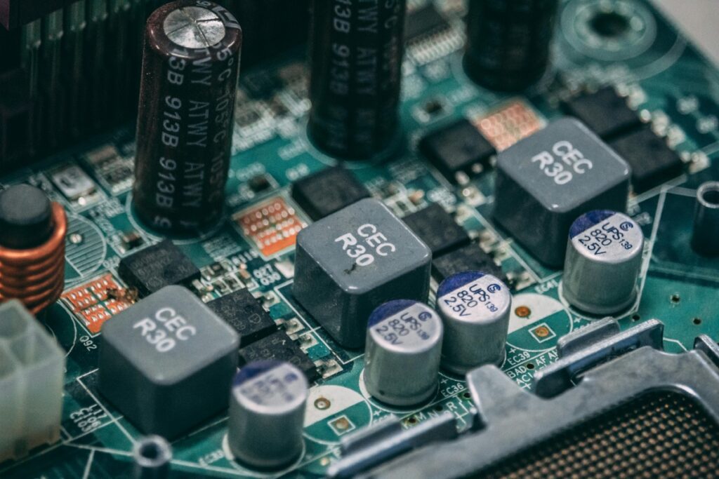
✅ Reliability: The Difference Between Good and Great Design
A PCB that “works” isn’t necessarily reliable. Over time, poor material choices, incorrect layouts, or weak solder joints can cause premature failures.
🚨 Key reliability factors:
- Board material: Choose the right PCB substrate for durability and thermal performance.
- Layer count: A single-layer board might be more reliable than a poorly designed multi-layer PCB.
- Component placement: Poor layout can lead to excessive heat, EMI issues, and mechanical stress.
2. Practical PCB Layout Tips That Make a Difference
🚀 Optimize Signal Flow
Think of your PCB design like a well-planned highway. You need clear lanes for signals to prevent congestion (interference).
🔹 Best practices:
✅ Keep AC/DC, high/low frequency, and high/low voltage traces separated.
✅ Avoid circular routing—straight traces with minimal turns improve performance.
✅ Isolation is key: Place analog and digital circuits on separate areas of the PCB.
⚡ Grounding is More Important Than You Think
Poor grounding is a silent killer in PCB designs. It’s one of the most discussed (yet often misunderstood) topics in electrical engineering.
Common grounding mistakes:
❌ Mixing high-frequency and low-frequency grounds.
❌ Creating long return paths, leading to unwanted noise.
❌ Ignoring proper grounding in multi-layer PCBs.
💡 Solution:
- Use a single-point ground in low-frequency circuits.
- For high-frequency designs, multi-point grounding is more effective.
- Minimize impedance by using wider ground planes whenever possible.
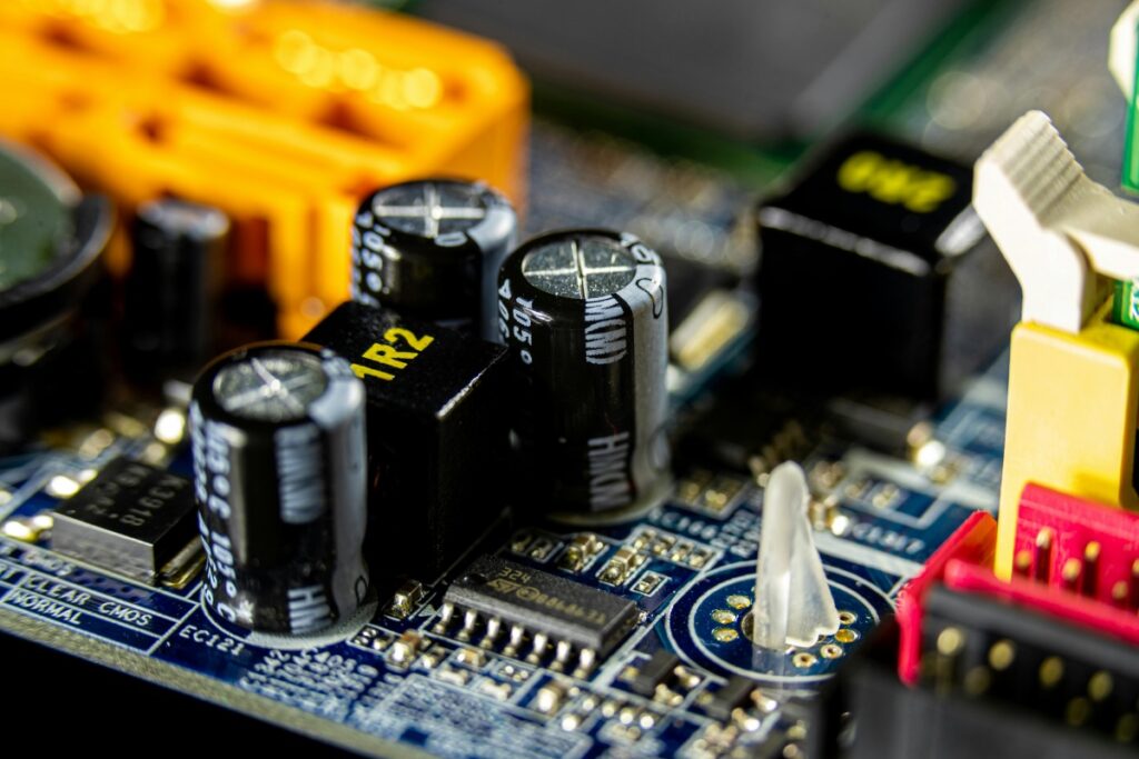
💡 Decoupling Capacitors: Don’t Just Place Them Anywhere
Many designers simply “scatter” decoupling capacitors across the PCB. This approach is ineffective!
Golden rules for decoupling capacitors:
- Place capacitors as close as possible to power pins.
- Use multiple values (e.g., 0.1µF + 10µF) for better filtering.
- Short, thick traces ensure lower impedance.
🚀 Bonus Insight: If your decoupling caps are properly placed, grounding issues become less noticeable!
🔧 Routing: Not All Traces Are Equal
- High-voltage and high-frequency traces must be rounded—avoid sharp corners.
- Power and ground traces should be as wide as possible to reduce resistance and improve stability.
- Avoid excessive vias—too many can lead to manufacturing defects.
3. PCB Printing & Manufacturing: Hidden Pitfalls
📌 Printing Settings Matter More Than You Think
Even if your design is flawless, poor printing can ruin everything.
🔹 Pro tips:
✅ Scale settings: Ensure 1:1 scaling to maintain design accuracy.
✅ Drill hole visibility: Enable “Show Hole” to ensure clarity for production.
✅ Layer selection: Be intentional about which layers to print—composite vs. single-layer prints matter.
🛠️ Avoiding Common Manufacturing Issues
- Too many vias = higher failure risk during production.
- Overly dense routing = soldering defects and bridging.
- Incorrect drill hole sizes = misalignment, poor solder connections, or broken pads.
4. Noise and Interference: Your Silent Enemies
🔊 Power and Ground Optimization
📌 Key principles:
- Keep power and ground lines as short as possible to minimize resistance.
- Align power and signal routing to reduce EMI.
- Use copper pours on empty PCB areas to improve grounding.
🛡️ Shielding Against Interference
- Separate analog and digital grounds to reduce noise coupling.
- Use ferrite beads on power lines to suppress high-frequency interference.
- Twist differential pair signals (like USB or HDMI) for better signal integrity.
5. The Art of Efficient PCB Layout: Practical Design Rules
🛠️ Key Routing Strategies
✅ Avoid parallel input and output lines to prevent signal coupling.
✅ Use 45-degree trace bends instead of 90-degree turns to improve signal flow.
✅ Optimize solder pad sizes—too small and they weaken, too large and they cause solder bridging.
💡 Practical Insights from Experience
- When designing for high-frequency applications, shorter traces are always better.
- Always check for thermal relief pads to avoid soldering defects.
- For multi-layer PCBs, dedicate a full layer to ground.
Conclusion: What 20 Years in PCB Design Have Taught Me
PCB design is both a science and an art. The difference between an “okay” design and a truly optimized PCB comes down to practical experience and attention to detail.
🚀 Key Takeaways:
✅ Correct design is the bare minimum—reliability and efficiency separate great designs from the rest.
✅ Signal integrity, grounding, and noise control are more important than just making connections.
✅ Manufacturability matters—if a PCB is difficult to produce, it’s not a good design.
✅ Testing and iteration are part of the process—expect to refine your designs multiple times.
🎯 Final Thought: Whether you’re a beginner or a veteran, there’s always something new to learn in PCB design. Stay curious, keep refining your skills, and never stop experimenting!